Silicon Carbide Electronics and Sensors
Enabling intelligence in the harshest aerospace environments.
SiC Electronics & Sensors Overview
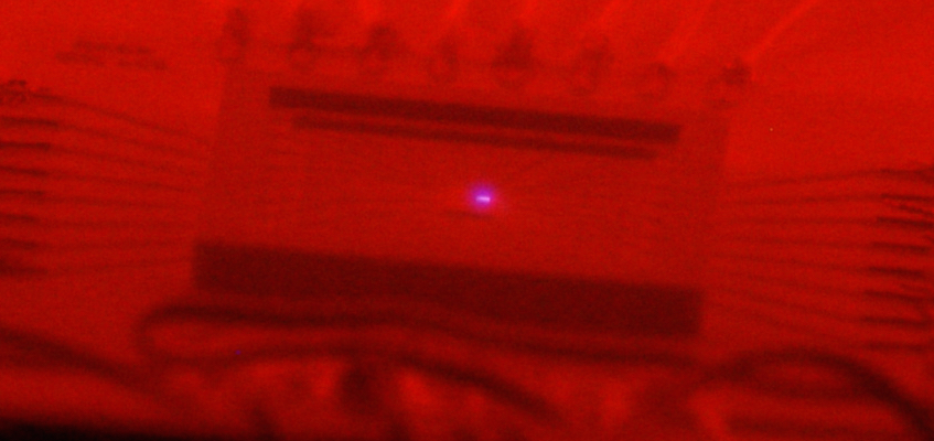
The NASA Glenn Research Center Smart Sensing and Electronics Systems Branch is developing silicon carbide (SiC) for beneficially bringing intelligent sensing and control electronic subsystems into harsh aerospace conditions (including 600 °C = 1112 °F glowing red hot!) beyond the physical reach of silicon technologies. Silicon carbide’s ability to function in high temperature, high power, and high radiation conditions will enable important performance enhancements to aircraft, spacecraft, power, automotive, communications, and energy production industries.
SiC Research at NASA Glenn
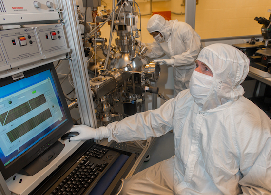
NASA Glenn Research Center continues to build on its pioneering SiC electronics history that dates back to the growth of singe-crystal layers as the foundation of early SiC diode and transistor demonstrations. NASA Glenn SiC technology advancements contributed to what is now an established global industry for SiC wafers and energy-efficient power devices for conventional application temperatures (of less than 200 °C). Today’s NASA Glenn SiC research is focused on implementing first-prototype SiC sensors and integrated circuits that will durably function for years in much more extreme aerospace environments (including 500 °C). These uniquely durable SiC devices are built in the NASA Glenn Microsystems Fabrication Laboratory starting from commercially purchased SiC wafers. This research is also concurrently advancing the packaging and testing needed to validate and deploy these new intelligent sensors and ICs into extreme application environments.
Work With NASA Glenn SiC Technology
Could your system benefit from sensors and integrated circuits (ICs) durably operating for years in the most extreme environments?
Given that accessibility and commercialization are key to new technology infusion, NASA Glenn prototypes developmental SiC IC designs for interested external partners, and is also exploring transition of manufacturing to commercial wafer foundries. The NASA Glenn 500 °C Durable JFET IC Technical User Guide is intended to stimulate further exploratory design, simulation, and layout of potentially beneficial application-specific ICs by new potential technology users. This User Guide should enable competent electrical engineers to design their own SiC integrated circuits for possible implementation in the next NASA Glenn developmental run.
If you are interested in working with or licensing NASA Glenn SiC electronics and sensors technology, please contact Jeanne King of the NASA Glenn Research Center Tech Transfer Office (216-433-2095).