Microsystems Fabrication Laboratory
Design, Fabrication, Packaging, and Testing of Uniquely Durable Extreme Environment Silicon Carbide (SiC) Sensors and Electronics
Facility Overview
The NASA Glenn Microsystems Fabrication Laboratory (MFL, located in Building 77) is a vertically integrated silicon carbide (SiC) semiconductor research and development facility dedicated to design, fabrication, and testing integrated circuit electronics and sensors uniquely durable to extreme environments. To date MFL is the only laboratory in the world that has fabricated and tested packaged semiconductor integrated circuits operating at 500 °C for over a year. This laboratory is available for assisting external partners in the design and prototyping of developmental extreme environment SiC sensors and electronics under mutual agreement negotiated by the NASA Glenn Technology Transfer Office. The MFL is comprised of multiple laboratories whose major equipment and capabilities are summarized below.
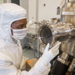
Cleanrooms
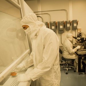
Approximately 3000 square feet of ISO 5 & 6 cleanroom space is employed for the fabrication of uniquely durable prototype SiC semiconductor integrated circuit electronics and sensors. These cleanroom laboratories execute the vast majority of the semiconductor batch fabrication processes needed to transform a commercially purchased SiC starting wafers into patterned arrays of completely functional SiC sensors and electronics. The images below highlight some of the key cleanroom equipment employed for prototype extreme environment device fabrication.
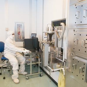
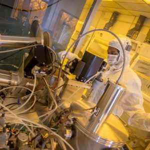
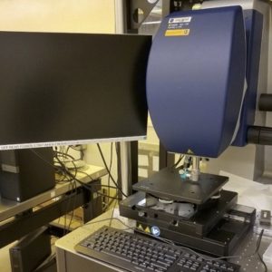
Fabrication Equipment
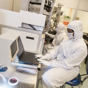
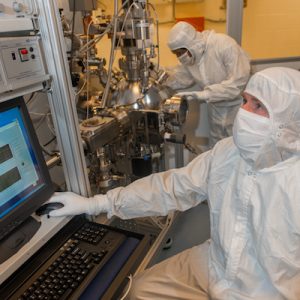
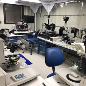
Characterization Equipment
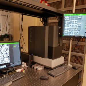
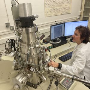
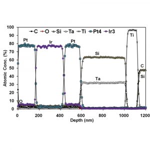
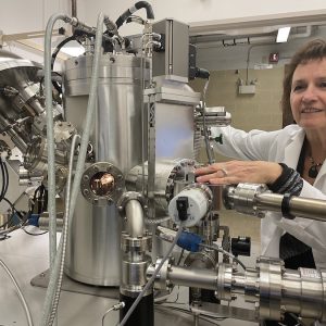
Surface Analysis
Development and fabrication of the SiC sensors and electronics are supported by surface analysis and materials characterization capabilities. The Surface Analysis Lab consists of X-ray Photoelectron Spectroscopy (XPS) and Auger Electron Spectroscopy (AES). These techniques provide surface composition, contaminant identification, and oxidation state information, as well as depth profiling from the surface into the bulk for a better understanding of reactions occurring during the fabrication process and high temperature testing.
Packaging
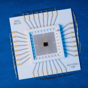
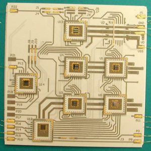
NASA Glenn Microsystems Fabrication Laboratory also carries out custom ceramic packaging of its uniquely durable SiC electronics and sensors chips. There are multiple wire bonders, wire-bond pull-strength and die-shear strength testers, and two saws for dicing fabricated SiC wafers chips, as well as equipment for accomplishing die attachment of SiC chips into ceramic packages in addition to assembly of multi-chip ceramic circuit boards for prolonged operation at 500 °C.
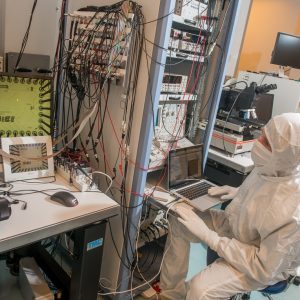
Electrical Testing
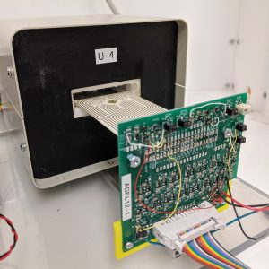
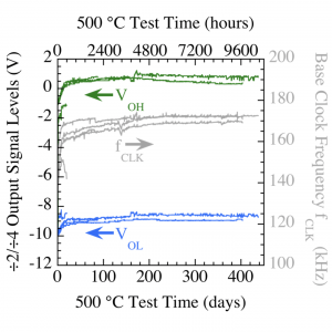
The NASA Glenn Microsystems Fabrication Laboratory is equipped to carry out prolonged automated electrical testing of packaged SiC integrated circuits and multi-chip circuit boards at 500 °C (as well as short-term electrical testing at even higher temperatures). This laboratory is presently undergoing a major expansion that will enable simultaneous prolonged 500 °C electrical testing of 32 chips in parallel including thermal cycling.
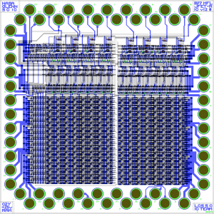
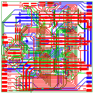
Design and Simulation
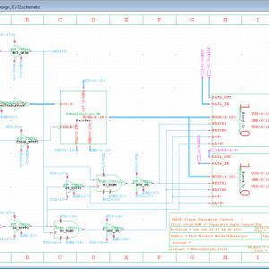
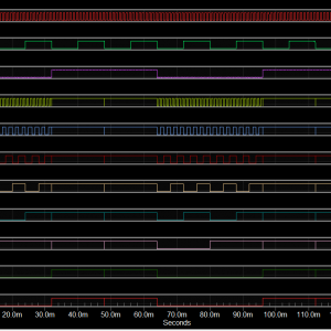
A combination of commercially available computer aided design (CAD) software tools has been adapted to the NASA Glenn SiC extreme environment process technology which facilitates efficient design, simulation, layout, and verification of integrated circuit (IC) designs as well as high temperature multi-chip circuit boards. Digital, analog, and mixed signal circuits are designed and simulated to function from -190 °C through +500 °C without significant input/output voltage changes. Electrical SPICE models and mask layout rules for SiC extreme environment IC design and simulation are posted online at https://go.nasa.gov/jfetic.
Facility Work
Most of the unique technology development work conducted in the NASA Glenn Microsystems Fabrication Laboratory is summarized on the NASA Glenn Silicon Carbide Electronics and Sensors website.
Contact
If you are interested in working with or licensing SiC electronics and sensors technology being developed in the NASA Glenn Microsystems Fabrication Laboratory, please contact Jeanne King of the NASA Glenn Research Center Tech Transfer Office (216-433-3132). This laboratory is available for assisting external partners in the design and prototyping of developmental extreme environment SiC sensors and electronics under mutual agreement negotiated by the NASA Glenn Technology Transfer Office.